Energy bands are the continuous ranges of allowed electron energies that form when many atoms bond into a crystal. The whole conductor/insulator/semiconductor distinction comes down to one thing: whether, and how easily, electrons can reach a band where they’re free to move.
From discrete levels to bands
In an isolated atom, electrons can only occupy specific, discrete energy levels, sharp rungs on a ladder. Bring atoms close together to form a crystal and the levels of neighbouring atoms interact and split. With the huge number of atoms in a real crystal (), the split levels pack so densely that each original level smears into a near-continuous band of allowed energies. Between the bands lie forbidden gaps: energy ranges with no electron state at all, so no electron can have an energy lying in the gap.
Two bands matter for conduction:
- Valence band — the highest band normally full of the bound, bonding electrons. Electrons here are locked into covalent bonds and can’t carry current.
- Conduction band — the next band up. An electron promoted into it is no longer tied to a particular bond and is free to move under an applied field, i.e. it can carry current.
Whether a material conducts is decided by whether electrons can get into the conduction band.
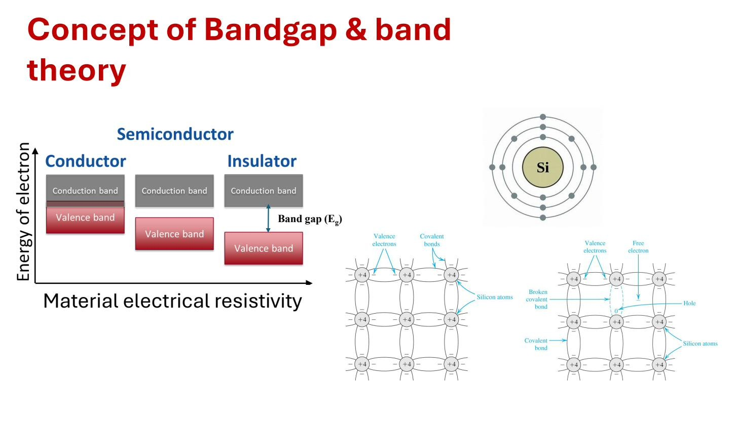 Conductors have overlapping/zero-gap bands, insulators a wide gap, semiconductors a moderate gap eV for silicon; a broken Si bond yields a free electron and a hole.
The three cases
The deciding quantity is the gap between the top of the valence band and the bottom of the conduction band, the Bandgap :
- Conductor: the valence and conduction bands overlap (zero gap). There are always electrons in the conduction band, with no energy needed to get them there. The material conducts strongly at any temperature.
- Insulator: the gap is large (several eV). At ordinary temperatures the thermal energy available to an electron ( at room temperature) is nowhere near enough to lift one across the gap. Almost no conduction-band electrons exist, so the material conducts nothing.
- Semiconductor: the gap is moderate, about for silicon. At room temperature a small but non-zero number of electrons happen to have enough thermal energy to jump the gap, so the material conducts weakly on its own and strongly once doped.
What a jump leaves behind
When an electron is promoted from the valence band to the conduction band, by heat, light, or a broken covalent bond, it leaves an empty state in the valence band. That vacancy is a hole, and it behaves as a mobile positive charge: neighbouring valence electrons can hop into it, moving the vacancy in the opposite direction. So a single band-to-band excitation creates a pair, one free electron plus one hole, the starting point for carrier generation and every semiconductor device that follows.