A memory cell is the smallest unit of digital storage, one bit. Memory chips are arrays of millions or billions of these cells, organized into rows and columns and addressed by their position.
The number of transistors per cell is the main design choice for a memory technology. It sets:
- Density: bits per square millimeter of silicon. Fewer transistors per cell → more cells per chip.
- Speed: fewer transistors usually means faster access (less capacitance to charge/discharge).
- Cost: fewer transistors means cheaper to manufacture per bit.
- Volatility: whether the cell loses its data when power is removed.
These trade-offs give the range of memory technologies in modern systems:
| Type | Transistors per cell | Speed | Density | Volatile |
|---|---|---|---|---|
| SRAM on-chip (L1/L2/L3, regfile) | 6 (8T/10T for multi-ported register files) | sub-ns | Low | Yes |
| SRAM discrete chip | 6 | ~10 ns | Low | Yes |
| DRAM | 1 + capacitor | ~50–100 ns access (much faster column burst) | High | Yes |
| ROM | 1 (mask ROM: half the cells have no device) | read fast | High | No |
| Flash | 1 floating-gate transistor | slow write, fast read | High | No |
Both SRAM rows use the same 6T cell. What changes between on-die cache and a commodity SRAM chip is the surrounding circuitry: on-die cells are tiny and sit next to fast sense amps tuned for short-wire local communication, while a discrete SRAM has to drive board-level signals at ~10 ns.
Every technology trades off some properties to get others. SRAM is fast but expensive per bit, so we use it for caches. DRAM is dense but slower, so it’s main memory. ROM and flash are non-volatile, so they’re for boot code and storage.
Cell organization on a chip
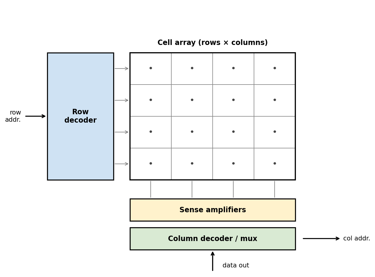 The standard array organisation: a row decoder activates a word line, every cell in that row dumps its value onto a bit line, sense amplifiers boost the small signals, and the column decoder picks which column’s value reaches the data output.
A memory chip arranges cells in a 2D array. To access one cell:
- Address bits split into row address and column address.
- The row decoder selects one row; all cells in that row are activated, dumping their values onto column lines (sense amplifiers boost the small signals).
- The column decoder selects which column’s value goes to the data output (or, for a write, which column receives the data input).
For example, a 128 K × 8 SRAM chip ( bytes, 8 bits each) has cells total in a array. Of the 17 address bits, the upper 10 select the row and the lower 7 select one of subgroups of 8 bits within the row.
This organization keeps the address pin count low: a 128 K chip needs only 17 address pins on the package, not 17 separate decode lines.
Why cell type defines memory class
The physical cell technology decides what the memory is good for:
-
6-transistor SRAM: needs constant power but holds its value as long as power is on. Each cell is a small flip-flop. Fast because it’s all transistors with no charge-decay issues. Used everywhere we need speed: registers, cache, fast SRAM chips.
-
1-transistor + capacitor DRAM: stores charge on a tiny capacitor, gated by one transistor. Cheap and dense. The catch: capacitors leak. The cell must be refreshed every few milliseconds (read and rewritten) or it loses its data. The refresh logic is built into modern DRAM chips.
-
Floating-gate flash: stores charge on an electrically isolated gate. Charge stays for years without power, but writing requires high voltages and slowly wears out the cell.
Different tiers of the Memory hierarchy use different cells because the trade-offs fit different roles.