A field-programmable gate array (FPGA) is a chip filled with a sea of small configurable logic blocks, surrounded by configurable interconnect, that can be programmed in the field to implement arbitrary digital circuits. Unlike a PLA or PAL, it doesn’t have an AND-plane / OR-plane structure. Instead it gives you a 2D fabric of logic blocks plus a routing network connecting them.
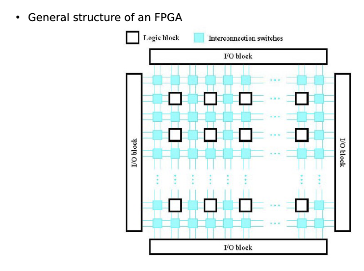
Three resource types make up an FPGA:
- Logic blocks — small programmable units, each capable of computing a Boolean function of a few inputs. Current FPGAs (Xilinx 7-series and later, Intel Stratix/Cyclone V and later) use 6-input LUTs plus flip-flops per block. Older parts (Xilinx Virtex-II, Spartan-3) used 4-input LUTs; “4–6” covers the historical span but the current standard is 6.
- I/O blocks — programmable pins that handle voltage levels, drive strengths, and direction.
- Interconnection wires and switches — the routing fabric that lets you wire any output from any logic block to any input on any other logic block.
The combination is a fully reconfigurable digital chip. A given FPGA might implement an Ethernet MAC today and a video codec tomorrow, by reloading its configuration bitstream.
Why this structure
Compared to PLAs:
- No fixed AND/OR planes. Each LUT can implement any function of its inputs (SOP, POS, XOR, parity, whatever you can write in a truth table of 4 to 6 inputs).
- Distributed logic. The same chip area can implement many small functions in parallel rather than one big two-level circuit.
- Routing flexibility. The programmable interconnect means you don’t need a pre-planned connection topology. The synthesis tool decides where each signal lives and routes accordingly.
This makes FPGAs much more flexible than PLAs, at the cost of being slower than custom silicon (ASICs) for the same function. Typical use cases: prototyping, low-volume products where an ASIC would be too expensive to design, signal processing where dedicated hardware is faster than software, and reconfigurable computing.
Programming flow
You write the design in VHDL or Verilog, run it through a synthesis tool that maps it onto LUTs, flip-flops, and routing, and the tool outputs a bitstream. Loading the bitstream into the FPGA configures every LUT’s contents and every routing switch, and within milliseconds the chip behaves as your circuit.
The bitstream is normally held in volatile SRAM, so the FPGA needs reloading at every power-up (usually from an attached flash chip). Some FPGA families use one-time-programmable antifuse or non-volatile flash configuration instead, trading reconfigurability for power-on speed.