A NAND gate outputs the complement of an AND: only when all inputs are .
| 0 | 0 | 1 |
| 0 | 1 | 1 |
| 1 | 0 | 1 |
| 1 | 1 | 0 |
Drawn as an AND symbol with a small bubble at the output. The bubble is the negation, same convention as a NOT gate.
 Image: NAND gate symbol, Public domain — distinctive-shape NAND gate (ANSI/IEEE 91-1984): AND body with an output bubble.
CMOS implementation
A 2-input NAND uses 4 transistors: 2 PMOS in parallel (pull-up network) and 2 NMOS in series (pull-down network).
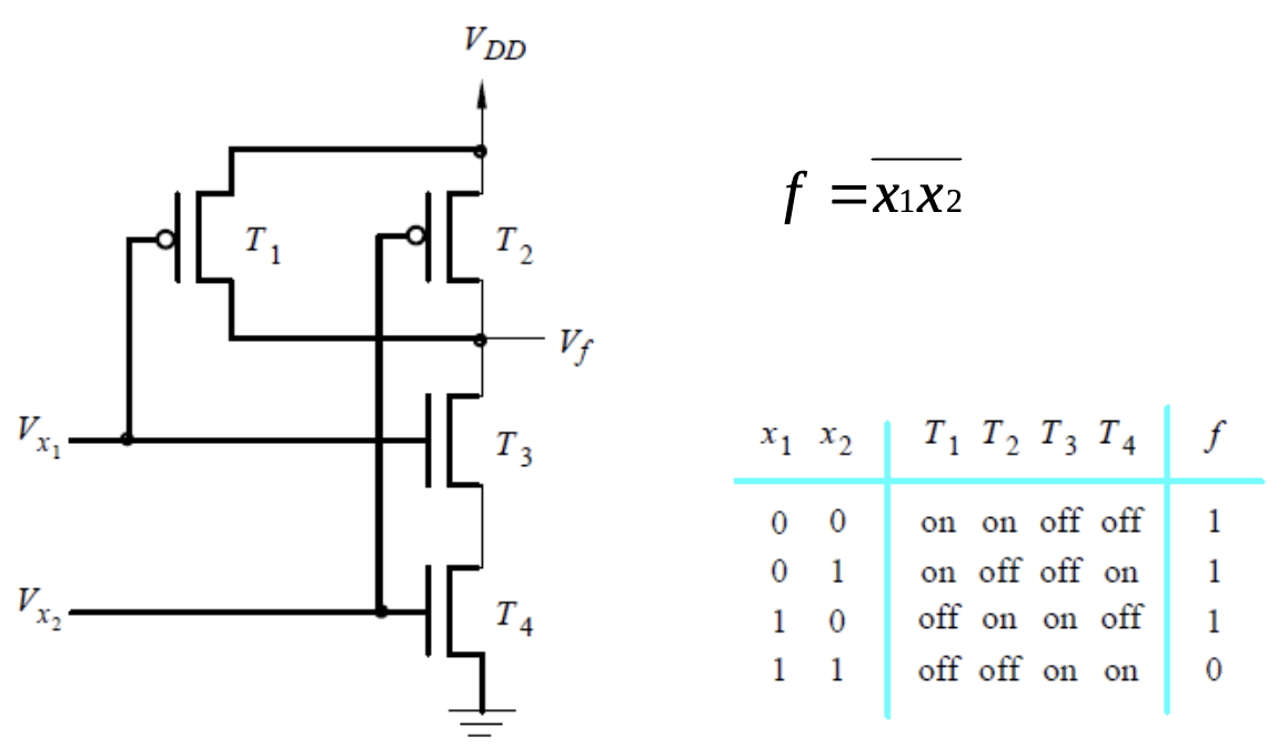
The pull-down chain conducts only when both NMOS are on (both inputs ), pulling the output low. For any other input combination, at least one PMOS in the pull-up is on (because at least one input is , turning a PMOS on), and the output is pulled high.
This is the natural way CMOS implements AND-like behavior. To get a true AND, you tack a NOT after the NAND, which costs another 2 transistors. NAND is cheaper than AND in CMOS.
Universality
NAND is a universal gate: any Boolean function can be built from NAND alone. The basic conversions:
- NOT: tie both NAND inputs together: .
- AND: NAND followed by NAND-as-NOT: .
- OR: invert both inputs (each via NAND-as-NOT) then NAND them: by De Morgan’s Laws.
This is why NAND gates are sometimes the only primitive in a fabrication library; everything else is composed from them. Compare with NOR gate, which is also universal but uses series PMOS (slower).
NAND-NAND synthesis
Any SOP expression can be converted directly to an all-NAND implementation:
- Write in SOP form.
- Apply double negation: .
- Push the inner negation into the OR using De Morgan’s Laws — each AND term becomes the NAND of its literals, and the outer OR becomes a final NAND.
Result: two layers of NAND gates, one for each AND term and one to combine them. Same structure as the original AND-OR circuit, just every gate replaced by a NAND.
Useful identities:
- — OR by NAND-ing the inverted inputs (De Morgan).
- — recover an AND by inverting a NAND.
- — OR built entirely from NAND, using NAND-as-NOT to invert each input first.