CMOS (Complementary MOS) is a logic family that uses both NMOS and PMOS transistors arranged so the output is always actively driven and never draws steady-state current. Every CMOS gate has two halves: a pull-up network (PUN) of PMOS transistors that connects the output to when the function should be , and a pull-down network (PDN) of NMOS transistors that connects the output to ground when the function should be .
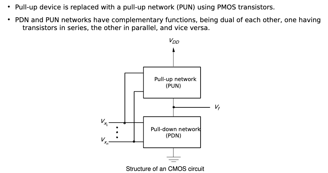
The two networks are complementary: for any input combination, exactly one of them is conducting and the other is off. So there’s never a path from to ground through the gate (no static current), and the output is always tied to either supply or ground (no floating outputs).
The two networks
The PUN and PDN are dual graphs: each network is built from the same input variables, but with the topology swapped. Every series connection in one network becomes a parallel connection in the other, and vice versa. Each network expresses, by its conduction condition, the function it pulls toward:
- The PDN’s conduction condition is the function that the gate should drive low. If the PDN conducts when , the gate output goes low when .
- The PUN’s conduction condition is the function that the gate should drive high. By De Morgan’s laws applied to the dual graph, the PUN conducts exactly when the PDN does not.
So if the PDN is ” AND ” (two NMOS in series), the PUN is ” OR ” (two PMOS in parallel, the dual graph). When , both NMOS conduct and pull the output low; both PMOS are off so the pull-up disconnects. For any other input combination, the NMOS chain is broken and at least one PMOS conducts, pulling the output high. This is exactly a NAND gate.
The mnemonic: in either network, stacked → AND’ed, parallel → OR’ed describes that network’s conduction condition. Because the gate output is the complement of the PDN’s conduction (and equals the PUN’s conduction), stacked NMOS in the PDN gives a NAND output, not AND.
Why CMOS dominates
Three properties combined make CMOS the default for digital chips:
-
No static power. Steady-state current is essentially zero. Current flows mainly during switching, both to charge or discharge load capacitance and from a brief shoot-through when both networks momentarily conduct as the input crosses the threshold region. So a CMOS chip dissipates power roughly proportional to its switching activity, not to its size.
-
Strong output drive. Outputs are always pulled hard to a rail, giving full-rail swings ( to ) and excellent noise margins.
-
Symmetric switching. With matched PUN and PDN, rise times and fall times are similar.
The price is that you need both transistor types, which costs silicon area. A CMOS NAND has 4 transistors; an equivalent NMOS-only ratio’d circuit would have 2 plus a load resistor, but that resistor wastes power continuously. The trade-off is worth it.
Building gates from PUN/PDN
To design a CMOS gate for a given function :
- Write in SOP form, that’s what the PUN naturally implements.
- The PDN implements . Derive it via De Morgan’s Laws from the PUN, replacing series with parallel and vice versa.
- NMOS goes in the PDN, PMOS in the PUN. Inputs feed both networks.
The result: a direct AND in CMOS is awkward (the natural pull-down is NMOS in series, which inverts the function), so AND is normally built as NAND-then-NOT. Same with OR (NOR-then-NOT). The “natural” CMOS gates are NOT, NAND, and NOR, and from those everything else.
| Gate (n-input) | CMOS transistors |
|---|---|
| NOT | 2 (1 PMOS, 1 NMOS) |
| NAND | |
| NOR | |
| AND | (NAND + NOT) |
| OR | (NOR + NOT) |
| XOR | ~8 |
| XNOR | ~10 |
XOR and XNOR are expensive in CMOS, which is why arithmetic circuits like adders try to use them sparingly. The exact transistor counts for XOR/XNOR depend on the implementation style (static CMOS, transmission-gate, pass-transistor) and are commonly quoted as 8–12.
Fabrication note (Electronics I)
“Complementary” is also a statement about silicon: CMOS builds both complementary device types (n- and p-channel MOSFETs) on a single chip. The n-MOSFETs sit directly in the common p-type substrate, while the p-MOSFETs are fabricated inside isolated n-type wells (n-wells) diffused into that substrate, so each transistor type has the substrate polarity it needs.