A NOR gate outputs the complement of an OR: only when all inputs are .
| 0 | 0 | 1 |
| 0 | 1 | 0 |
| 1 | 0 | 0 |
| 1 | 1 | 0 |
Drawn as an OR symbol with a bubble at the output.
 Image: NOR gate symbol, Public domain — distinctive-shape NOR gate (ANSI/IEEE 91-1984): OR body with an output bubble.
CMOS implementation
A 2-input NOR mirrors a NAND gate structurally but with the networks swapped: 2 PMOS in series in the pull-up, 2 NMOS in parallel in the pull-down.
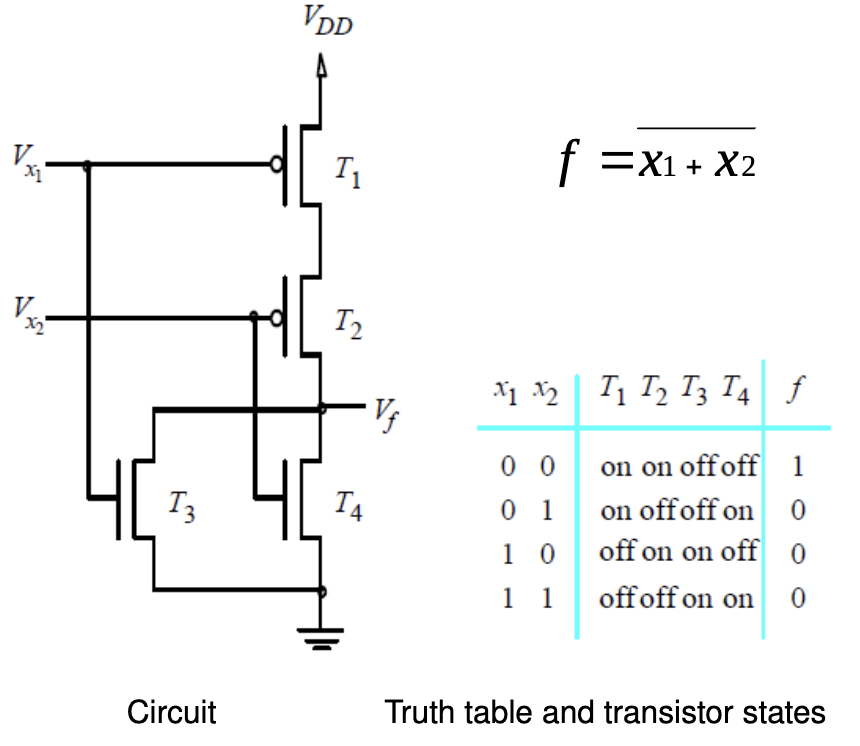
The pull-up chain conducts only when both PMOS are on (both inputs ), pulling the output high. For any other combination, at least one NMOS in the pull-down is on, dragging the output low.
In silicon NOR is slower than NAND for the same logic depth, because the series PMOS chain has more resistance than a series NMOS chain (holes are slower charge carriers than electrons). When designers have a choice, they prefer NAND-based logic. NOR is the better fit when the natural expression of a function lends itself to it, like the cross-coupled latch, which is built from two NORs.
Universality
NOR is also a universal gate — any Boolean function can be built from NOR alone, just like NAND.
Conversions:
- NOT: .
- OR: NOR followed by NOR-as-NOT: .
- AND: invert both inputs via NOR-as-NOT, then NOR: by De Morgan’s Laws.
NOR-NOR synthesis
Dual to NAND-NAND synthesis. Convert a POS expression to an all-NOR implementation:
- Write in POS form.
- Apply double negation and push the inner negation into the AND using De Morgan’s Laws. Each OR term becomes the NOR of its literals, and the outer AND becomes a final NOR.
Useful identities:
- — AND by NOR-ing the inverted inputs (De Morgan).
- — recover an OR by inverting a NOR.
- — AND built entirely from NOR, using NOR-as-NOT to invert each input first.
Pick NAND-NAND for SOP-style designs and NOR-NOR for POS-style designs. Either works for any function; the difference is which form has fewer terms after minimization.