A logic gate is a physical implementation of a Boolean operation. Inputs and outputs are voltages, usually (“low,” logical ) and (“high,” logical ), and the gate’s transistors are wired so the output voltage equals the Boolean function of the input voltages.
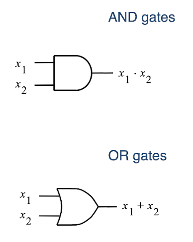
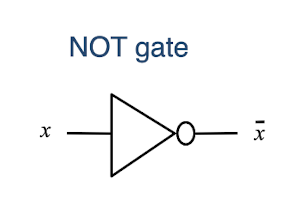
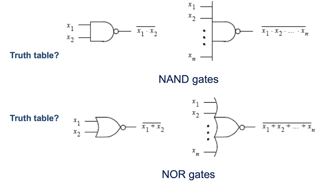
The standard schematic symbols:
The basic family is AND (Conjunction), OR (Disjunction), and NOT (Negation). From these you build the derived gates: NAND gate, NOR gate, XOR, XNOR.
How to read the symbols
- AND is the D-shape with a flat back. Output high only when all inputs high.
- OR is the curved-back shape with a pointed front. Output high if any input is high.
- NOT is a triangle pointing toward its output. The small bubble at the tip is the negation marker.
- A bubble anywhere on a gate (input or output) means “invert at this point.” NAND is AND with an output bubble. NOR is OR with an output bubble.
The bubble notation lets you redraw a circuit to make its function obvious. By De Morgan’s Laws, a NAND gate is equivalent to an OR with bubbles on both inputs, so the symbol can be drawn either way depending on which form makes the design clearer.
Fan-in
The number of inputs a gate accepts is its Fan-in. Real gates have practical limits (typically 4–6 inputs in CMOS) before propagation delay and power dissipation get too bad. A 12-input AND is usually built from a tree of smaller ANDs.
Implementation
In modern silicon every gate is some arrangement of NMOS and PMOS transistors (see CMOS for the full pull-up / pull-down structure). A NOT gate uses two transistors, a NAND uses four, a NOR uses four. AND and OR are usually built as NAND-NOT or NOR-NOT pairs because wiring a “true” AND directly in CMOS gives a worse circuit.