Once you have a small-signal model of a three-terminal transistor, there are exactly three single-transistor amplifier topologies, distinguished by which terminal is held common (AC-grounded) to both input and output. Each has its own combination of voltage gain, input resistance, and output resistance, and picking the topology is the design decision. The MOSFET and BJT versions are direct analogues, differing in one detail that traces to a single physical fact.
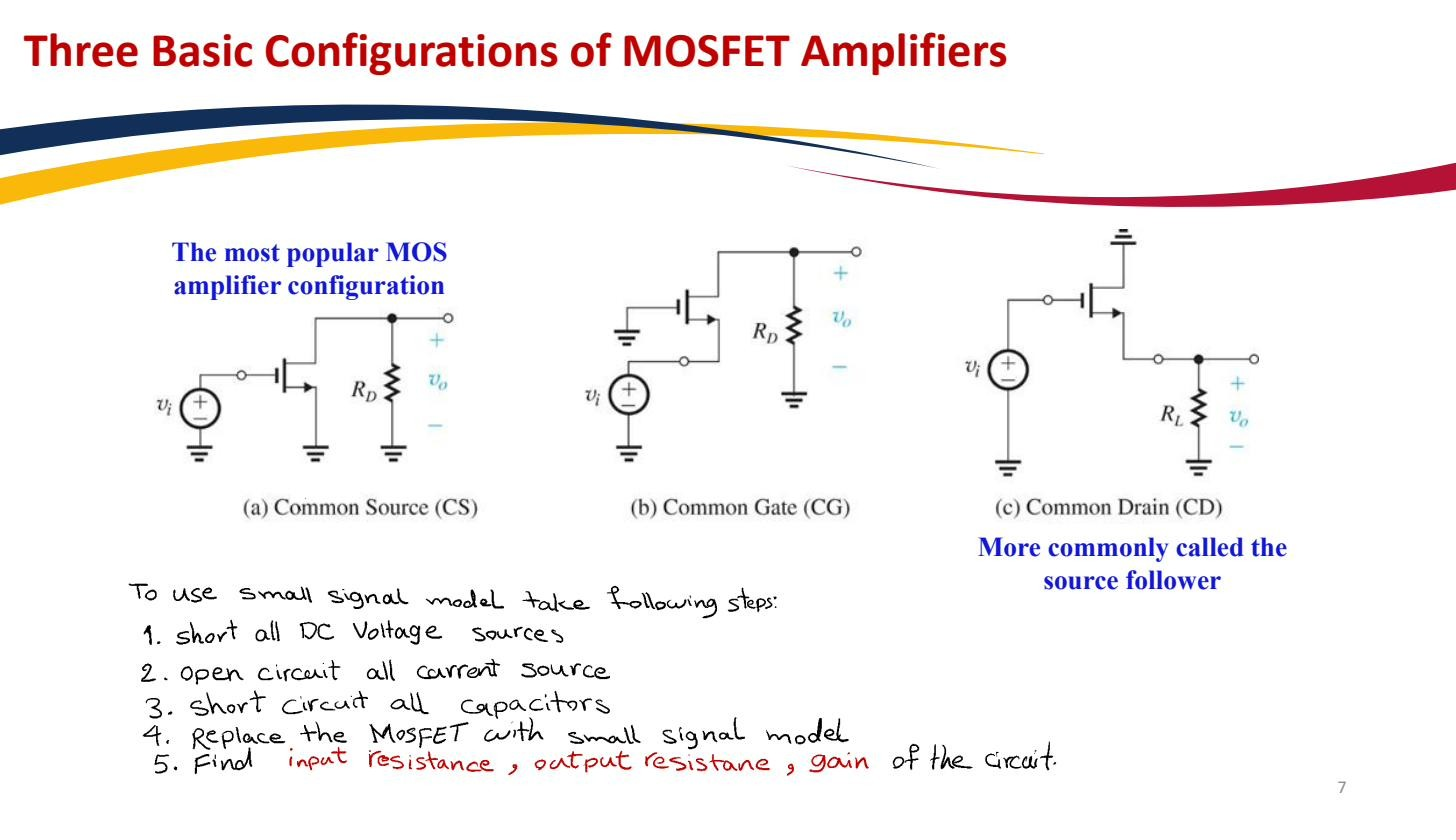 The three MOSFET configurations: common-source, common-gate, common-drain.
The three patterns
Common-source / common-emitter — input at gate/base, output at drain/collector, source/emitter common. High voltage gain, inverting (), moderate input and output resistance. The default voltage amplifier; reach for it first. Gain for the MOSFET. See Common-source amplifier and Common-emitter amplifier.
Common-gate / common-base — input at source/emitter, output at drain/collector, gate/base common. Voltage gain similar in magnitude to CS/CE but non-inverting, low input resistance, high output resistance. It doesn’t give you more gain. What you get is the low input resistance (it acts as a current buffer: current in at the source comes out at the drain almost unchanged) and good high-frequency behaviour, since it sidesteps the Miller effect. Used at high frequency and as a current buffer. See Common-gate amplifier and Common-base amplifier.
Common-drain / common-collector — input at gate/base, output at source/emitter, drain/collector common. These are the Source follower and Emitter follower. Voltage gain (just under), high input resistance, low output resistance. No amplification, but it transforms impedance. The Buffer amplifier that goes at the output of a chain to drive a heavy load without the gain stage sagging.
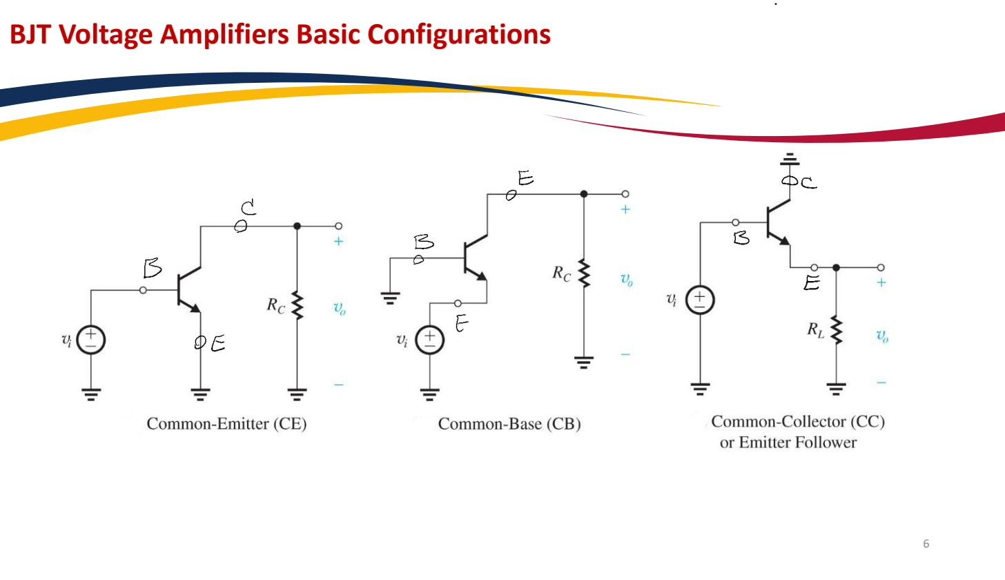 The three BJT configurations: common-emitter, common-base, common-collector, the direct counterparts.
Why MOSFET and BJT versions differ at all
Every difference between the MOSFET and BJT families traces to one fact: the MOSFET gate draws no DC current (the gate is insulated by the Gate oxide, so is an open circuit at DC), whereas the BJT base draws . That makes the BJT’s small-signal input resistance finite (, looking into the base) while the MOSFET’s is effectively infinite (looking into the gate). Everything else (bias-network design, the input-resistance formulas, why BJT stages load preceding stages and MOSFET stages do not) follows from this. Learn the three patterns once and the device just sets whether is finite or infinite. Input and output resistance (amplifier) covers why and are the quantities that decide which topology a given job needs.