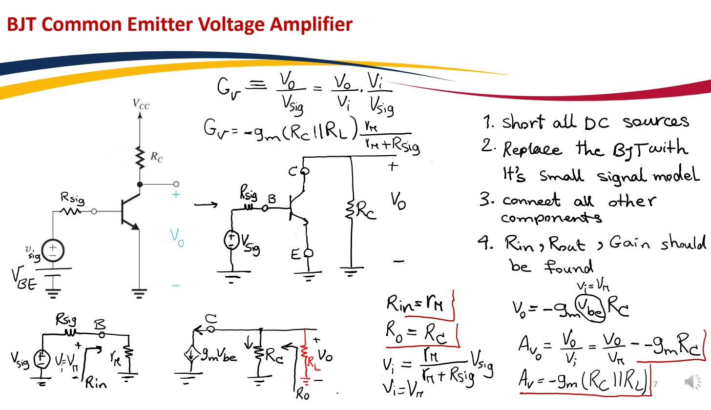
The common-emitter amplifier is the workhorse single-transistor BJT voltage amplifier: input at the base, output at the collector, emitter held at AC ground. It’s the BJT analogue of the Common-source amplifier with the same qualitative properties: high gain, inverting, the default voltage-amplifier stage.
Why it amplifies
Bias the BJT in active mode at an operating point (see BJT DC analysis), then superimpose a small signal on the base–emitter voltage: . In active mode the device is a voltage-controlled current source, so the small signal produces a collector-current change
where is the BJT transconductance. That current flows through the collector resistor , and the output is the collector voltage. Because flowing into the collector pulls the collector voltage down,
The minus sign makes the stage inverting: a 180° phase shift between input and output. The transistor turns an input voltage into a current via , and the resistor turns that current back into a much larger output voltage.
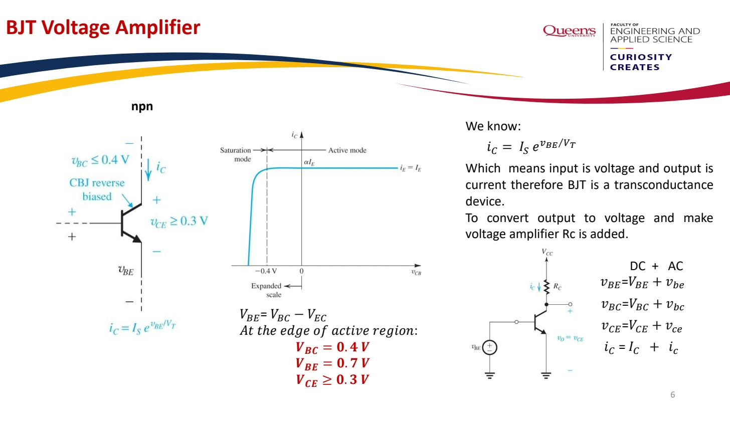 BJT voltage amplifier topology: , where is the DC bias and the small signal; the output swings about its DC bias as varies.
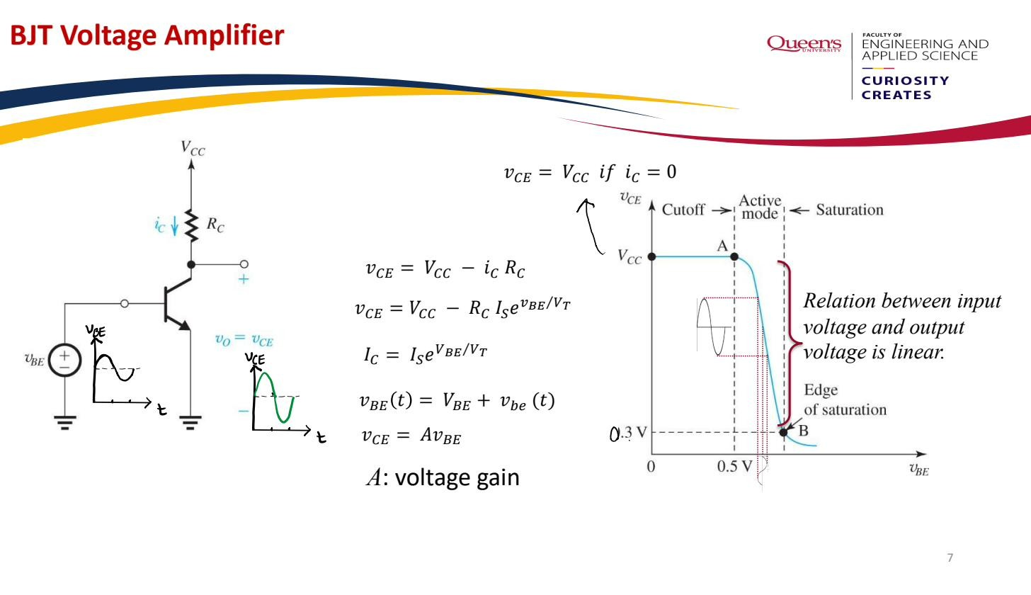 swings inversely with the input , the source of the inversion.
Gain by differentiating the transfer characteristic
The same result drops out of the large-signal transfer characteristic. The output is with (BJT collector current). The small-signal gain is the slope of versus at the bias point:
using . Same answer two ways: the linearised current model and the slope of the DC transfer curve agree, as they must.
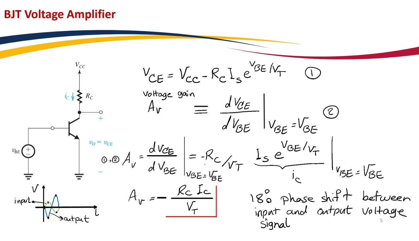 Derivation: ; the minus sign means the output is inverted (180° phase shift).
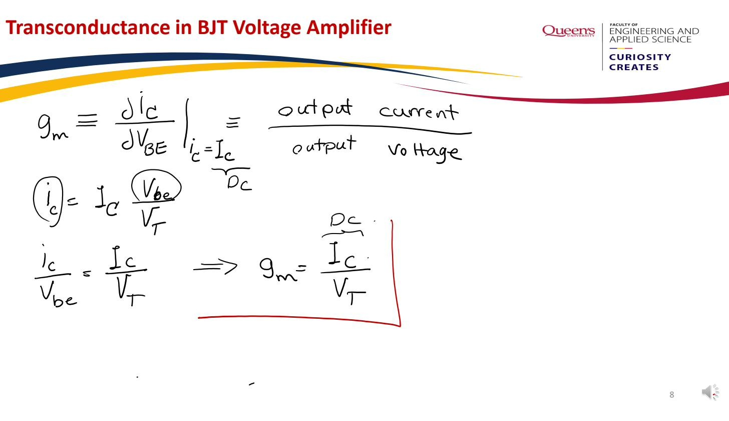 Detailed analysis of the BJT amplifier transconductance and output voltage.
Input/output resistance and the Early-effect ceiling
- Input resistance: , the BJT input resistance, finite (a few kΩ). This is the main weakness versus the infinite-input-resistance MOSFET stage.
- Output resistance: , looking back into the collector.
Including the transistor’s own output resistance from the Early effect, the collector load is , so the more complete gain is
This is why sets a hard ceiling on how much gain a single CE stage can produce. The input and output resistances matter once stages are cascaded.
 The most useful BJT amplifier configuration: high gain, inverting.
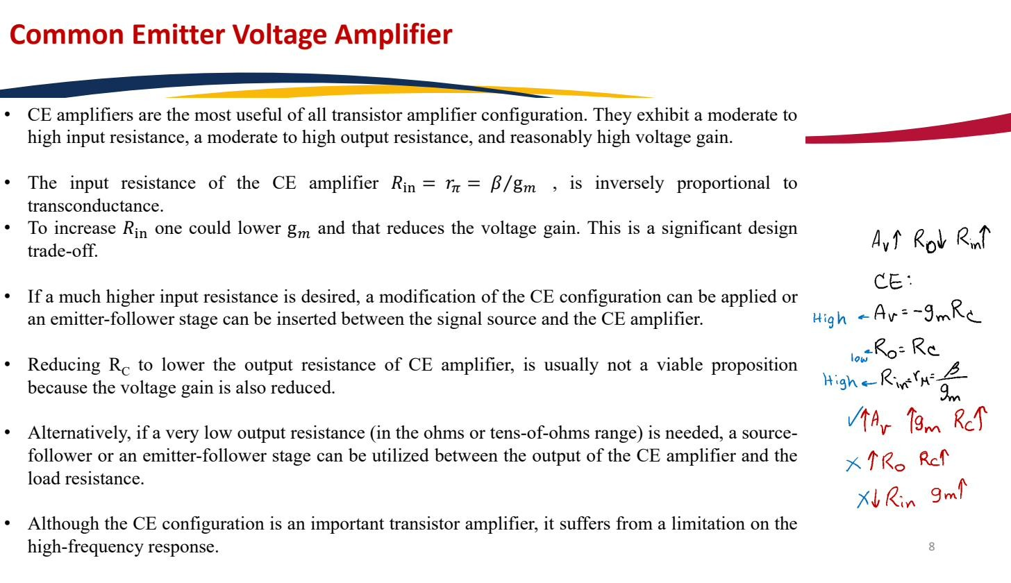 CE amplifier characteristics: high voltage gain, moderate input resistance, moderate output resistance, signal inversion.
To trade some of this large gain for predictability and bandwidth, add an un-bypassed emitter resistor (Emitter degeneration). The full board-level realisation with biasing and coupling capacitors is the Discrete-circuit BJT amplifier.