A bipolar junction transistor (BJT) is a three-terminal amplifying device built from two pn junctions placed back-to-back, sharing a thin middle region. First transistor ever built (Bell Labs, 1947), and dominated electronics for decades before the MOSFET took over digital logic. It survives in analog design because its transconductance per unit current beats a MOSFET’s and because well-matched pairs are easy to fabricate, which matters for instrumentation and precision analog work.
Structure: three regions, two junctions
A BJT has three regions of alternating doping type stacked together. Cross the device and you pass two metallurgical junctions. The two flavours are npn (n-type emitter, p-type base, n-type collector) and pnp (p-type emitter, n-type base, p-type collector). They’re written up separately as NPN transistor and PNP transistor because their bias polarities differ, but the physics is the same with carriers and voltages mirrored.
The three terminals are:
- Emitter (E) — heavily doped; its job is to emit (inject) carriers into the base. The arrow in the circuit symbol is always on this terminal.
- Base (B) — the thin, lightly-doped middle region. “Thin” is literal: under one micron in a modern device. It controls the device the way the gate controls a MOSFET, but unlike a gate it draws a small current.
- Collector (C) — moderately doped and physically the largest region; it collects the carriers that survive the trip across the base.
The two junctions are named after the regions they separate:
- Emitter–base junction (EBJ) — the pn junction between emitter and base.
- Collector–base junction (CBJ) — the pn junction between collector and base.
The whole behaviour of the device comes down to which way each of these two junctions is biased: see BJT operating modes for the four combinations.
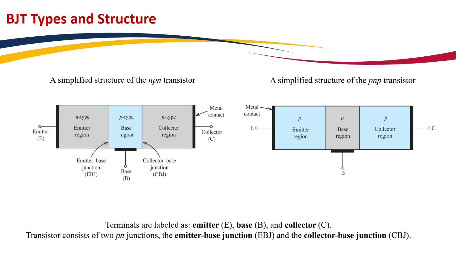 npn (left) and pnp (right): three regions of alternating doping type form two back-to-back pn junctions, the emitter–base junction (EBJ) and the collector–base junction (CBJ).
Why the base must be thin and lightly doped is the structural fact everything else hangs on. In active mode the emitter floods the base with carriers; if the base were thick or heavily doped, those carriers would recombine before reaching the collector and the device would be useless. A thin, lightly-doped base lets almost all of them diffuse straight across (see Minority-carrier injection). This deliberate asymmetry is also why the emitter and collector are not interchangeable even though both are the same doping type in an npn.
npn versus pnp, and why npn dominates
In an npn the working carriers are electrons; in a pnp they are holes. Electrons have higher mobility than holes, so an npn is faster than a pnp of identical geometry and is the default device in modern circuits. All the worked analysis here uses npn devices; the pnp is the polarity-reversed mirror image, exactly as a p-channel device mirrors an n-channel MOSFET.
Compared with a MOSFET the BJT trades the MOSFET’s near-infinite input resistance (the gate draws no current) for a much steeper exponential i–v law, and therefore a higher BJT transconductance and more current for the same bias. That trade is why BJTs persist in analog front-ends.
Circuit symbols
The symbol is two leads (collector and emitter) coming off a vertical bar (the base), with an arrow on the emitter lead. The arrow points in the direction of conventional emitter current in active mode:
- npn: arrow points out of the device (base → emitter). Mnemonic: “NPN — Not Pointing iN.”
- pnp: arrow points in (emitter → base).
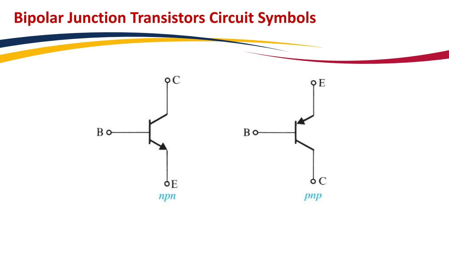 Arrow out for npn, arrow in for pnp. The arrow indicates the direction of conventional current flow in the emitter when the transistor is in active mode.
The defining electrical relationship, valid in active mode, is that the collector current is a fixed multiple of the base current: , where is the Common-emitter current gain (typically 50–100). Combined with KCL at the device, , this is enough to analyse most BJT circuits (see BJT DC analysis).