The operating point (Q-point, quiescent point, bias point) is the set of DC voltages and currents a device sits at with no signal applied. For a diode it is the pair ; for a MOSFET it is ; for a BJT it is . It is the point on the device’s – curve about which all signal behaviour happens.
How it is found
Find it by DC analysis: zero every signal source and solve the circuit with the device’s large-signal (non-linear) model, the Constant-voltage-drop model or Exponential diode model for a diode, the square-law equation for a MOSFET. This is Step 1 of Small-signal analysis. For the worked diode example with V, k, the CVD model gives the operating point from a single KVL equation.
The operating point matters because the small-signal parameters are evaluated at it. The Diode small-signal resistance is , so it depends entirely on where Q is. Move the bias current and you change the gain of every amplifier built around the device. The bias point is a design choice, not an afterthought.
Why Q must sit in the active region with room to swing
An amplifier only amplifies linearly if the device stays in its active region (saturation for a MOSFET, forward-active for a BJT, the steep forward part of the curve for a diode) throughout the entire signal swing. The signal rides up and down around Q. If Q sits too close to an edge of the active region, one side of the swing pushes the device out of it (into triode, cutoff, or saturation for a BJT) and the output clips: it flattens off instead of following the input.
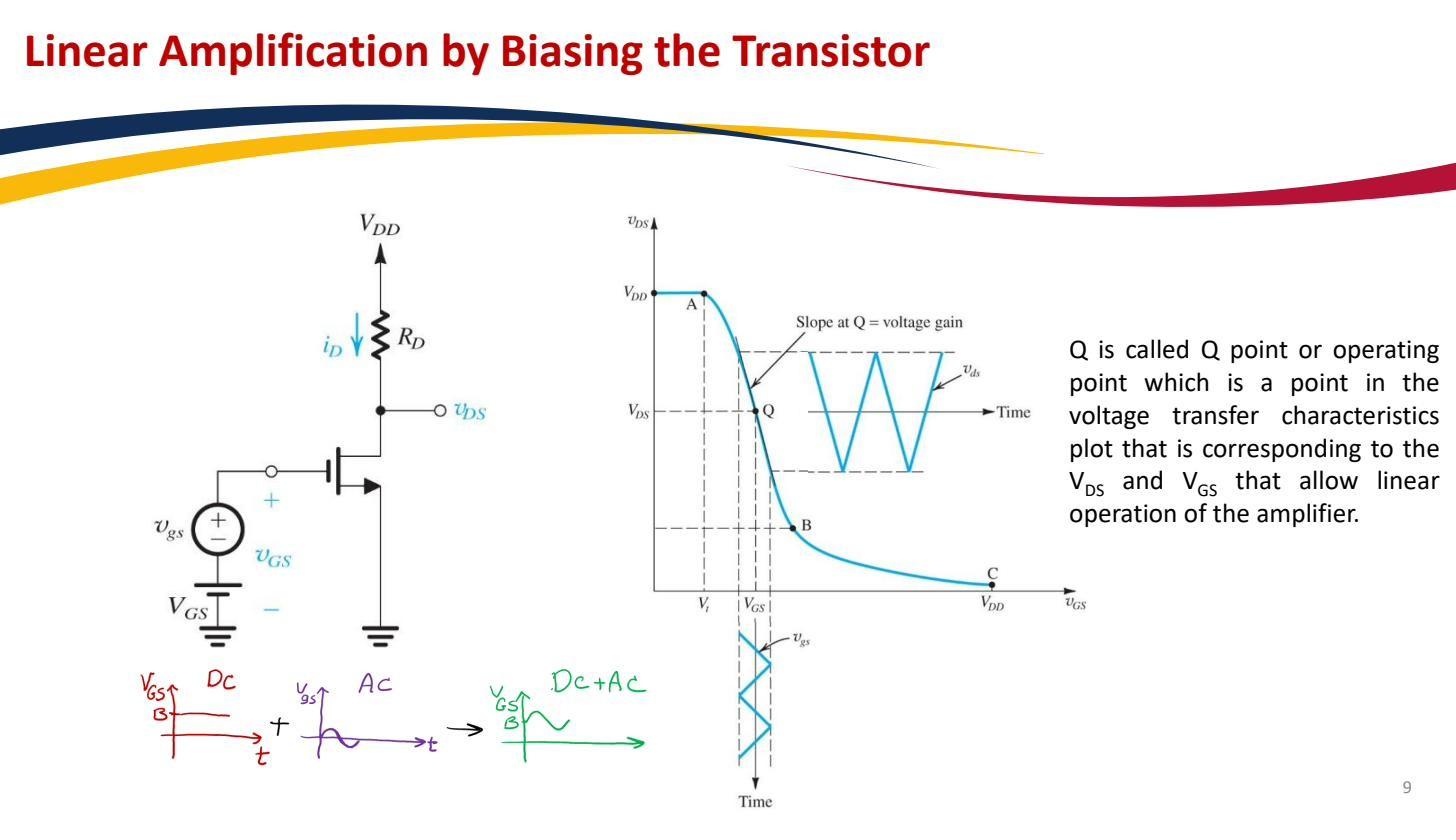 Choosing in saturation so the small-signal swing stays linear; placing near an edge clips the signal.
So a good operating point sits centred in the active region with enough headroom on both sides for the largest expected swing, and biased stably so component tolerances and temperature don’t drift Q into a bad spot. Choosing it well is the job of MOSFET biasing. As the input DC level varies, Q traces out the Voltage-transfer characteristic; its linear region is where Q must live.