A pn junction is what you get when p-type and n-type silicon are formed in adjacent regions of the same crystal. It’s the building block underneath every diode and every transistor in this course. The asymmetry in how it conducts (easily one way, almost not at all the other) is the property everything else is built on.
What happens when the two materials meet
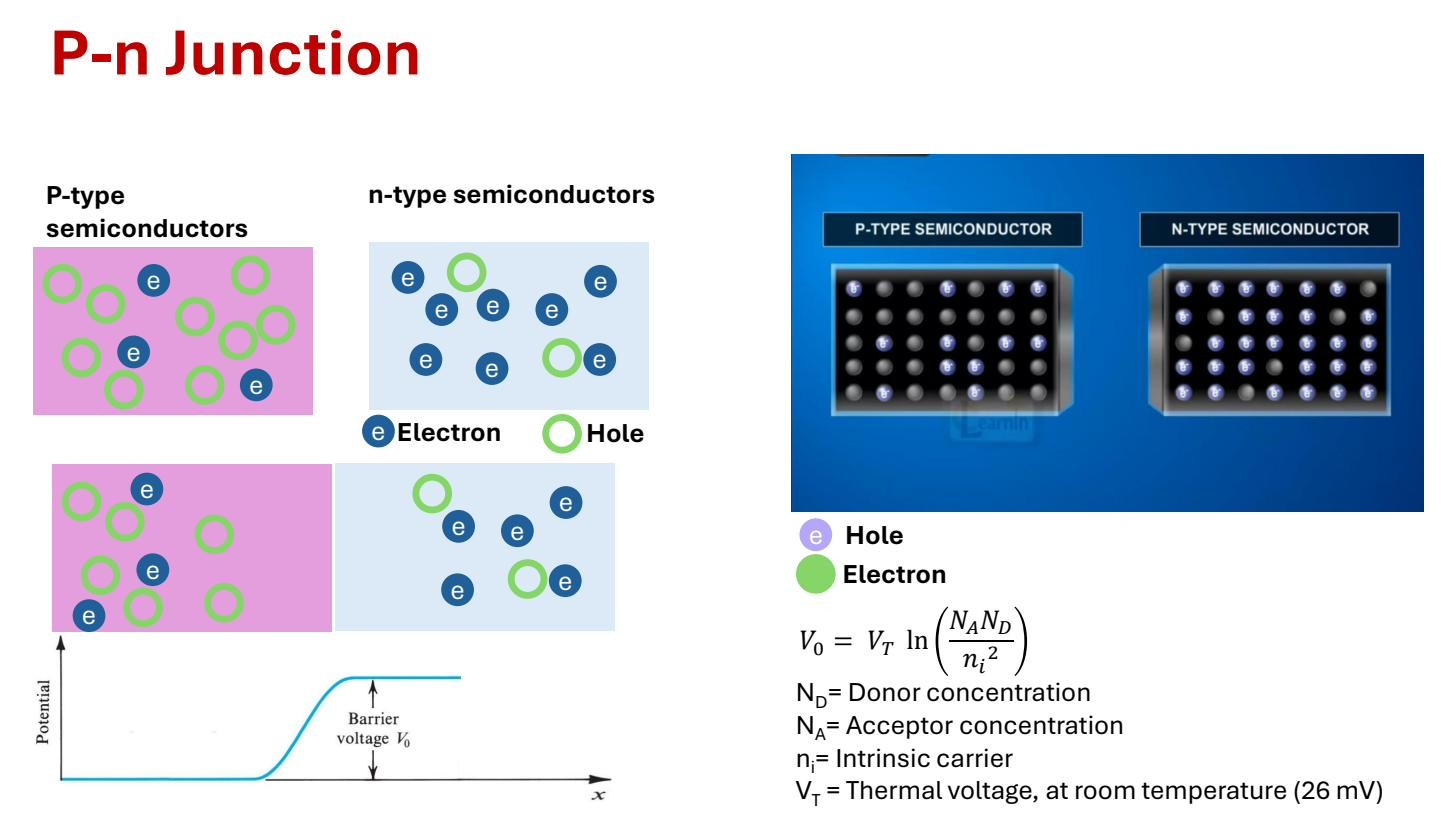
The n-side has a huge surplus of mobile electrons; the p-side has a huge surplus of mobile holes. Put them in contact and the concentration gradient drives diffusion: electrons spill from n into p, holes spill from p into n. Particles moving from where they’re crowded to where they’re not, same physics as a drop of ink spreading in water.
Each electron that leaves the n-side leaves behind a fixed, positively-charged donor ion locked in the lattice. Each hole that leaves the p-side exposes a fixed, negatively-charged acceptor ion. So a thin region straddling the junction fills up with immobile ionised charge: positive on the n-side, negative on the p-side. This is the space-charge (depletion) region, “depleted” because the mobile carriers have been swept out of it.
 Diffusion of carriers across the metallurgical junction leaves behind a space-charge region of ionised donor and acceptor atoms, creating a built-in electric field and a potential barrier .
The built-in field reaches equilibrium
That exposed ionic charge sets up an electric field pointing from the n-side to the p-side. The field pushes electrons back toward n and holes back toward p, so it opposes the diffusion that created it. As more carriers diffuse, the field grows, until the drift current it drives exactly cancels the diffusion current (see Drift and diffusion current). At that point net current is zero and the junction is in thermal equilibrium.
The stable potential difference left across the junction in equilibrium is the Built-in voltage . For silicon at room temperature . You can’t measure it with a voltmeter (the metal–semiconductor contacts at the ends of the device produce equal and opposite contact potentials that exactly cancel ), but it’s very real inside the device: a carrier crossing from n to p must climb an energy hill of height .
Biasing changes everything
Apply an external voltage and the equilibrium breaks (see Forward bias and Reverse bias):
- Forward bias (p to +, n to −): the applied voltage opposes , lowering the barrier to . Far more carriers have enough thermal energy to cross, and current grows exponentially with applied voltage. This is the Diode equation.
- Reverse bias (p to −, n to +): the applied voltage adds to , raising the barrier to . Almost no carrier can cross; only a tiny Reverse saturation current flows, carried by minority carriers.
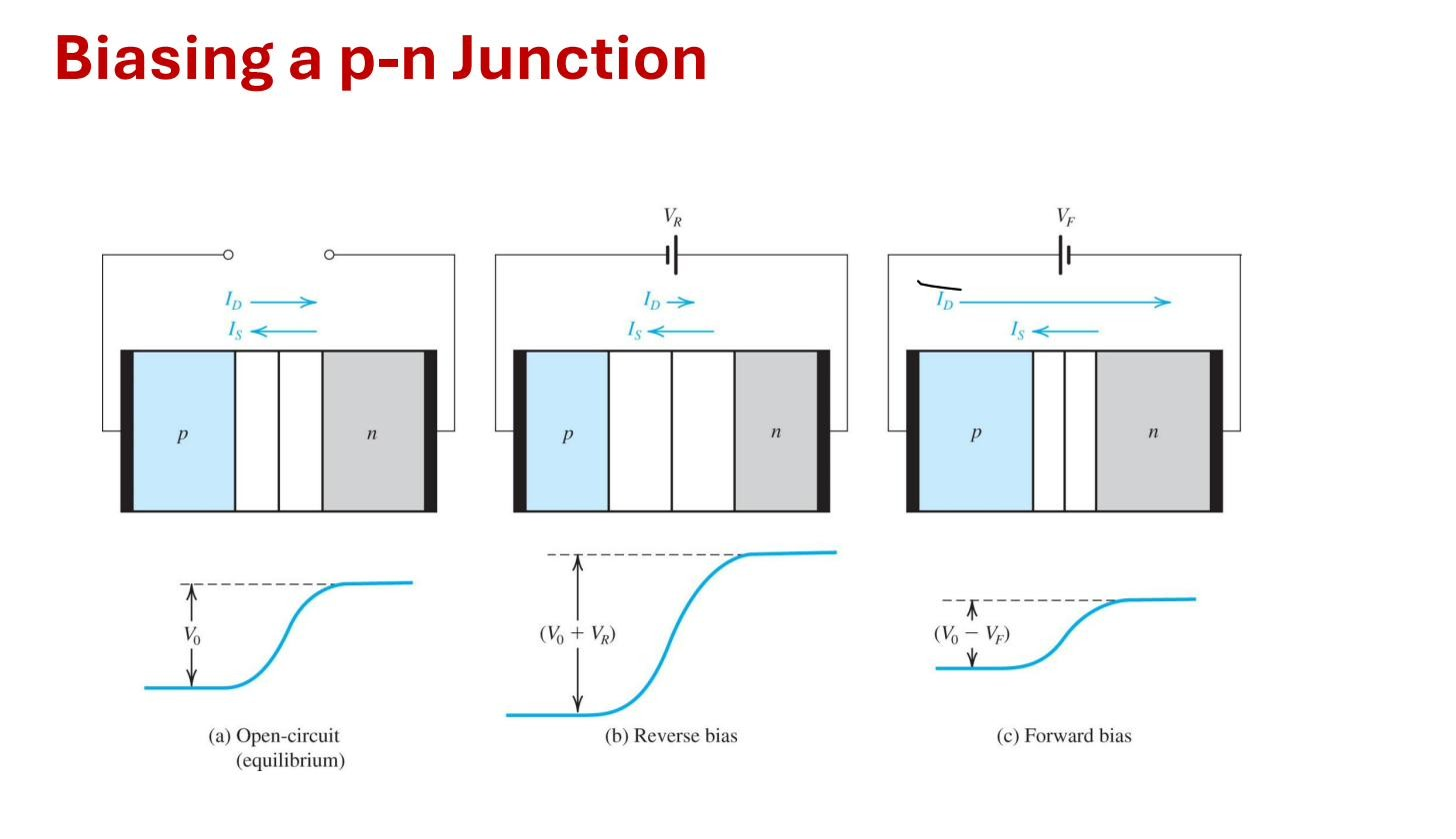 Forward bias lowers the barrier and lets a large diffusion current flow; reverse bias raises the barrier and blocks current.
That one-way-valve behaviour, large current in forward bias and negligible current in reverse, is the whole reason the pn junction is useful. The Diode chapter is just the details of this exponential – relation, and both the MOSFET and the Bipolar junction transistor are built from pn junctions used in these two regimes.