The gate oxide is the very thin layer of insulating silicon dioxide (SiO₂) that separates the conductive gate of a MOSFET from the silicon substrate beneath it. Its thickness is , typically only a few nanometres in modern processes.
The gate is a capacitor
The gate (metal or heavily-doped polysilicon) is one plate, the silicon under the oxide is the other plate, and the thin SiO₂ between them is the dielectric. That’s a parallel-plate capacitor, which is why no DC gate current flows. A capacitor passes no steady current (the oxide is an insulator), so the gate controls the MOSFET channel purely by the field it sets up across the oxide, drawing essentially zero current to do it. That’s why a Field-effect transistor presents a near-infinite input resistance and a Common-source amplifier has an essentially infinite input impedance.
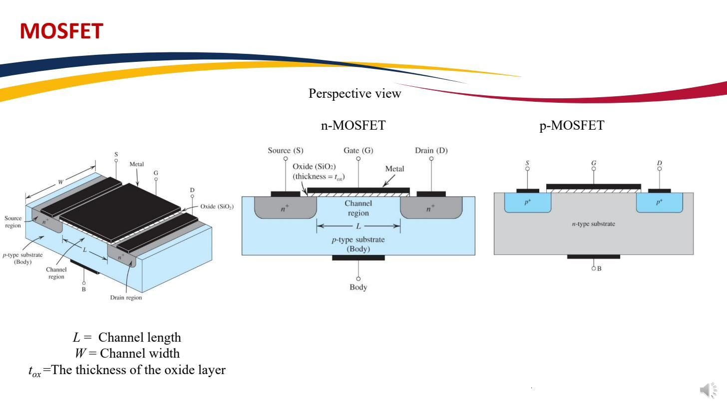 = channel length, = channel width, = gate-oxide thickness.
Oxide capacitance per unit area
The relevant quantity is the capacitance per unit area of the gate stack,
where is the permittivity of silicon dioxide and the oxide thickness. A thinner oxide means a larger : the gate plate sits closer to the channel, so the same gate voltage attracts more channel charge and the device is “stronger.” That’s why scaling MOSFETs to thinner oxides increases drive current.
feeds straight into the MOSFET transconductance parameter: the process transconductance is , where is the electron mobility in the channel. So the oxide’s geometry (, through ) directly sets how much drain current a given overdrive produces, through every drain-current equation. The other defining MOSFET dimensions are the channel length (source-to-drain spacing along the surface) and channel width (perpendicular to ); the device transconductance parameter is .